Highly Efficient 0-100% LED Dimmeror: How to convert 10mA from your battery into 20mA for your LED |
|
This webpage describes a highly efficient LED dimmer, or a dimmable LED flashlight, or a switching current source, or whatever you want to call it. Cheap, single-IC, uses commonly available parts, easy to build. Designed to get the longest light out of a (rechargable) battery, ideal in emergency situations: some 24+ hours for a single white LED at full brightness from a cheap 9V, 200mAh battery. Works well from 4 up to at least 30 Volts; may even vary over time, while the brightness level is maintained essentially constant. Can drive as many LEDs as would normally be possible with the given supply voltage. Efficiency up to 94% (*), or even higher when a cunningly split supply voltage system is used.
While I've been doing electronics for some 15-20 years, this happens to be my first web-documented project. That's because it's not quite trivial, it wasn't yet documented anywhere in this form, and it's potentially useful for more people than only me. Oh, and this project uses ideas from a variety of online sources, so "giving back" is also a motivation.
For this project, some prior experience with electronics is required. I will not answer your questions, sorry. Instead, the explanation below is very detailed indeed. I should probably issue a WARNING for that. On the other hand, if your day job is to design lighting systems for cellphones or the like, this page won't tell you much you didn't already know.
This project and webpage including all images are copyright © 2006 J.A. Bezemer, and are licensed under the terms of the GNU GPL ≥2. This basically means that you're very free to use and modify and re-publish it, as long as you also publish your source material (e.g. files from your schematics drawing program), and preferably include a back-reference to this webpage. And if you produce and sell anything based on this project or webpage, you will have to provide all gory details to your customers if they ask for it.
Oh, and before I forget: I cannot be held responsible for anything you do; there is no guarantee that any information on this page is correct (always use independent verification); avoid looking directly into bright LEDs; apply due caution when working with voltages >40V; all trademarks and registered trademarks mentioned on this page are the property of their respective owners. So, that should keep the lawyers happy.
(*): "Practically theoretical" value for the special case that the supply voltage is exactly enough to feed the LEDs at full brightness. The PWM then turns on continuously (100% duty cycle), giving a constant overhead current <1.2mA; LED current 20mA and only a trifle more loss in R7 and parasitic resistances.
Some basics of LED dimming
Let's start by looking at some LED circuits.
(Click on picture to open it in another window; handy while reading the long text below)
Starting simple
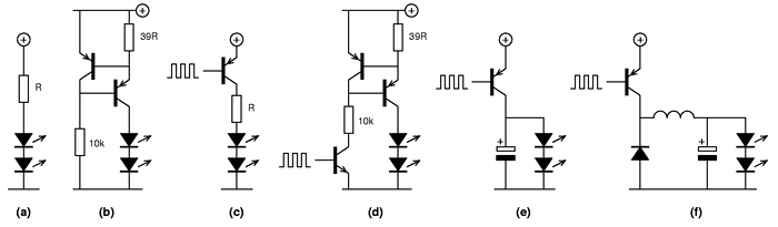
Circuit (a) doesn't need explaining. R depends on the number (and kind) of LEDs and the supply voltage, which isn't very handy if you want to be independent of either (or both). Oh, and if you don't know how to calculate R, this project is not for you.
To always have the same brightness independent of the number of LEDs and the supply voltage level (think nearly-empty batteries), a current source is a much better solution. Circuit (b) depicts one variant that I particularly like. I found it on the 4QD-tec website; circuit 4 there is the NPN variant. A simple explanation: imagine the upper-left transistor isn't there, then the middle-right transistor is fully turned on because its base is "connected" to ground. Now what the upper-left transistor does, is "steal" the ground level away from the middle-right's base -- but only if there's more than ~0.68V across the 39Ω resistor. This will effectively shut off the middle-right transistor in such a way that ~0.68V is always maintained across the 39Ω resistor. Voilà your current source of 0.68/39 = ~17.5mA. (Use 33Ω to get ~20mA, at which your expensive white LEDs have a guaranteed lifespan of only 1000 hours..!)
Adding dimmability
So, that's all good and well, but now for the dimming part -- that is, obtaining an adjustable brightness (i.e. current). One simple option is to use a transistor that gets turned on just enough to produce the desired current, possibly controlled by an opamp that monitors the voltage across a shunt resistor and compares that to a variable reference voltage. I didn't draw such a circuit because it sidesteps from our way to improvement.
The other way of dimming is by varying the time during which the LEDs are burning, rather than the current: Pulse Width Modulation or PWM. A high-frequency, 50% duty cycle square wave applied in circuit (c) causes the LEDs to "fake" half brightness, because the eye can't distinguish the very short full-on and full-off periods and just registers the average brightness.
Just for completeness, we can apply that same principle to circuit (b), for example giving circuit (d). If your PWM output goes high enough, you can forget the bottom-left transistor and connect the 10k resistor directly to the PWM output. Shown is the only circuit variant that will cut off all current during the off periods, but it's not necessarily the best choice. In particular, doing the switching with another PNP parallel to the top-left transistor may give some faster switching action.
Increasing efficiency
Both circuit (c) and (d) share the characteristic that a 100% PWM duty cycle (=always on) will cause the circuits to act just like their non-PWM counterparts -- i.e. power is consumed by the resistor and the current source. And that's the big problem with these circuits. For the highest efficiency, we want no resistive elements that consume power. Transistors are only okay if they're always either full-on (saturated) or full-off.
So, we take circuit (c) and just get rid of the resistor. It will still work, as long as the on-periods are very short indeed: say 5 µsec on at (guess) 200mA and 45 µsec off, which gives 5/(5+45) * 200 = 20mA average. Throw in a capacitor to smooth it out a bit, and we've got circuit (e). This immediately reminds us of a standard mains power supply in which, at the low-voltage side of the transformer, AC power is rectified and smoothed out by a capacitor; only in this case it's high-frequency spikes instead of the usual 50/60Hz sine wave. This works quite nicely, be it that monitoring the average current isn't the easiest thing to do.
However, the biggest problem in circuit (e) are the large spike currents. On the one hand, the LEDs probably won't like spikes of 200mA and even if they do, their light output doesn't grow linearly at currents above 20mA. This can be solved to some extent by a large enough capacitor. On the other hand, the large currents will certainly be too much for the switching transistor. Practically all high-gain transistors can only handle 100mA max, while high-current transistors usually have low gains which would require a relatively high control current (100% loss) to drive it into saturation.
The solution is to introduce an inductor or coil or choke into the circuit. Just like a capacitor ramps up to a certain voltage, an inductor ramps up to a certain current. And, just like a capacitor, it doesn't lose any energy (okay, okay, just a tiny amount due to the resistance of the long wire, but we will ignore that for the moment). Now we can leave the transistor on for a longer time, while the current ramps up from 0 to (say) 60mA. Oh, and we need the current to ramp down again, too... Remember from your standard relay circuit, that a coil will assume any voltage level so that it may lose its current "charge", which means that it will break the control transistor if it doesn't have any other choice. So, like in any relay circuit, we need to add a diode to the mix. We could just add it in parallel to the inductor, so that the latter can emtpy itself nicely on its own, but that's 60mA (ramping down) through the diode and ~0.68V across it, which gives... 100% loss. Now here is the very smart idea: add the diode in such way that the inductor loses its current through the LEDs. That's circuit (f).
More on the inner workings
Closer inspection of circuit (f) shows that, when the transistor is turned on, the inductor current flows from Vcc via the transistor and LEDs to ground. And of course the capacitor is still charged in the process, as it was in circuit (e). But when the transistor turns off (think: erased from the circuit), the current still present in the inductor can only flow down via the LEDs and back up through the diode. There's still some power loss in the diode, but most of the stored energy is now neatly converted into light by the LEDs. To stick some numbers on it: when the transistor is on, the inductor current ramps up from 0 to (say) 60mA, and when the transistor is off, the inductor current ramps down again from 60 to 0mA and stays there. And there's still the capacitor to smooth things out even more.
Actually, if the inductor is "large enough" (takes very long to charge and discharge), we can initially just leave the transistor on until the inductor current reaches 21mA, and subsequently start switching the transistor off and on again with such a frequency that the inductor current never leaves the 19-21mA region. This means that during the "on" periods, also the transistor current will be just 19-21mA. Now, if we "happen" to have realised this with a 50% duty cycle, then the average power supply current will be 50% of 19-21mA which is... 10mA.
To reach the highest possible efficiency, we should carefully choose all components to minimise power loss. Of course we need super-bright LEDs that produce the most light output per Watt electrical power. And we need a coil with reasonably thick wires so that its resistance is as low as possible. Also capacitors have some resistance (called "ESR"), because the plates are very thin and the dielectric material isn't perfect. In general, tantalum capacitors are a good choice, but they are expensive and usually limited in voltage range; add to that my experience which suggests that capacitor ESR usually isn't a problem at all. Then we have the transistor, which should be turned on fully, well into saturation, and also quickly enough. Finally, there is still the diode, the one component that loses the most power. In the last example above, it has 20mA flowing for 50% of the time, at a voltage of ~0.68V. The current is given and can't be reduced, but the voltage can go down quite a bit by choosing a suitable diode type. If your first thought is: "Now where did I leave those germanium diodes", then that probably shows your age and area of expertise. Nothing wrong with that, of course! It's just that germanium only has a low voltage for very low currents; at 20mA it can go to 1.5V and higher. The modern variant is the Schottky diode, with voltages less than 0.3V even at 100mA currents. Oh, and diodes also have some resistance, which is usually less with high-current versions.
Well, now we've been deriving and constructing a very well-known circuit and I didn't even mention its well-known name. Sorry for that. It's the buck circuit, of course. And it's a "Step-Down" DC-DC converter in the form of a Switch-Mode Power Supply (SMPS). Yet the nice thing is, you probably always found switch-mode stuff complex or even scary, while you now know that it's just plain simple PWM with a twist -- quite literally indeed. Oh, you already knew SMPSs? Then why are you even reading this?
As always, Google knows more about buck circuits.
Schematic and discussion
The LED dimmer is based on circuit (f) above, but it's quite a bit more complex since it also includes the PWM oscillator and the current sense/compare circuitry. And of course the reference voltage generation, which is a story of its own.
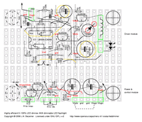
Here is the complete circuit diagram.
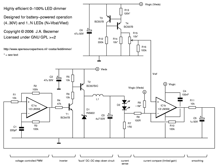
(Click on picture to open it in another window; PRINT the PostScript or PDF version; EDIT the original Xfig file with Xfig, also on Windows. Note: GNU GPL ≥2, so if you publish anything based on these files, you must also publish your own source files.)
We immediately notice the buck circuit as T2, D1, L1, C3 and D2. Everything else is needed to make the buck circuit work as intended. We also see two separate supply voltages, but for the moment just assume they are the same.
In this section, we'll look at the circuit only qualitatively. In the next section, we'll see why the exact component types and values were chosen as shown, and discuss some alternative options.
Note: datasheets are listed below.
Voltage-controlled PWM
Let's start at the left-hand side. A very compact voltage-controlled PWM circuit is formed by IC1a, R2, R3 and C1, with the control voltage applied via R1. I found this circuit as a Design idea in the EDN magazine (July 6, 2000, p. 136), also on page 2 of the PDF version (local cache). We happen to use the same component labels, only different values that work better with the different opamp type. The EDN's R4 resistor is only needed because the TLC393 has an open-drain output; our LM358 has a normal output so our R4 has a different purpose.
In case you don't want to read the detailed and formulaic explanation in the EDN article, here's the simple version. If the voltage across C1 is "too low", IC1a will have a high output and C1 will get charged via R3. If the voltage of C1 gets "too high", IC1a will flip to a low output and C1 gets discharged again by R3. Given a constant control voltage at the left-hand side of R1, the feedback via R2 will cause a schmitt-trigger-like threshold behaviour so that C1 actually has two different voltage levels to oscillate in between. The exact position of these voltage levels is determined by the control voltage applied via R1, and that way we can effectively choose which part of the well-known exponential charge/discharge curves of R3/C1 we want to use. With a low control voltage (thus low thresholds), we use the lower parts of the curves, which give rapid charge (on) and slow discharge (off), i.e. a low PWM duty cycle. With a high control voltage, it's the exact opposite. When the control voltage is tied to ground, IC1a will be locked in the discharge cycle, since the voltage across C1 can't get below ground level which would be needed to flip IC1a back on. Again the exact opposite happens with the control voltage tied to Vcc -- actually, it only needs to be equal to the maximum output voltage of IC1a itself (C1 can't be charged higher than that). So we have built ourselves a simple 0-100% PWM circuit.
The control voltage is automatically adjusted by the current sense/compare circuitry, so we don't need to think about that much more. One nice thing to mention is that the output of IC1b can go as low as ground and as high as... IC1a's maximum output voltage, so we indeed have the 0-100% PWM functionality available.
The PWM output of IC1a is first fed into a simple inverter T1, since the buck circuit's PNP transistor T2 requires an active-low input. One extra advantage is that this also "sharpens up" the on/off slopes, which is handy because the LM358 isn't the fastest guy in town. And another nice side effect is that this allows T2 to operate at a supply voltage different from that of the rest of the circuit; more about that later. Theoretically, R5 wouldn't be required, but it helps discharge the parasitic capacitance inside T2 at the on-off transistion, which makes it switch slightly faster. ("Fully on" and "fully off" don't waste power, but the short "half on" situation during transitions implies resistive behaviour and thus resistive losses.)
The buck circuit is the same as discussed above, so no need to explain that again.
Current sense and compare
The LED current is measured by a quite small-valued resistor; this is possible because the LM358's input range includes ground level (and even slightly below ground). The measured voltage, say 0.02V for 20mA, could be fed directly into the negative input of IC1b, but despite L1 and C3, the current still "wobbles" enough to make IC1b produce a quite large "wobble" at the output. That's why we not only reduce the gain by means of R8 and R10, but also smooth the "wobble" even more by means of R11 and C5. The result, after C5, is a nice steady voltage that's excellently suitable to control the PWM with.
An ideal opamp, when equipped with a useful feedback mechanism, is "omniscient" and will adjust its output to exactly that voltage level which will result in the voltages on its two inputs being exactly equal. In other words, reasoning the other way around, V+ is equal to V-, and Vout makes that so. In our case: set Vref to 0.020V and IC1b will do anything necessary to maintain a 20mA current through the LEDs. That's just what we want.
Only, opamps are not perfect. Most importantly in this context, they can't measure V+ and V- in exactly the same way. So, they will do anything to make V+ exactly equal to... V- plus or minus something (or vice versa, if you prefer). That "plus or minus something" is called the offset voltage. Normally you wouldn't even notice, but here we find that the LM358 has an offset voltage typically somewhere between -2mV and +2mV, which is really large if you're trying to compare 20mV voltage levels. For example, if you set Vref to 20mV, in reality IC1b may do anything necessary to maintain not 20, but 18mA current through the LEDs. Or, when the offset voltage happens to have the other polarity, not 20 but 22mA. Okay, you say, then I'll just change the range of Vref to either a slightly higher or a slightly lower maximum, and that'll take care of it. Indeed it does, but only at the high end. The low end is more problematic. In the first example a Vref of 0mV "should" produce a -2mA current through the LEDs, but that isn't possible so nothing is wrong there (just that the LEDs only start shining above Vref=2mV). But in the second example, Vref=0mV will still produce a 2mA current through the LEDs -- simply because that's the only way to obtain a 2mV level for V-, which IC1b thinks equals the 0mV level at the positive input. In other words, you won't be able to turn the LEDs fully off. That's not nice. So what we need to do, is "fake" a 2mV level at the negative input even when there's no LED current at all. That's what R9 does (together with R8-R7). 50% chance that your particular opamp doesn't need it, 50% chance that it does. And if it does need R9, the indicated value of 1MΩ is only a wild guess, maybe a higher value suffices (say 4.7MΩ), maybe an even lower value is required (say 470kΩ). The only way to know for sure, is to build the circuit and see what works best. Just to give you some data points: I've got 5 LM358s, two of which don't need R9, two are fine with 1MΩ, and one needs even less than 1MΩ.
Reference voltage
The big question for today is: how to generate a reference voltage which can be adjusted between 0.000V and 0.020V, irrespective of the supply voltage level (4..30V), while consuming practically no current at all.
The first thougt would probably be to use a zener diode or just a forward-biased normal diode, with a resistor to Vcc that limits the current to a very low value (say, 0.1mA). For a normal diode, this would give a voltage between 0.5 and 0.6V; include a potentiometer (in series with a suitably large resistor to get the voltage down) alongside the diode, and it will work just fine. But first of all, you'd notice that the reference voltage varies quite a bit with the supply voltage, because a (zener) diode tends to act almost like a resistor at these low current levels. And second, you'd realise that all current through the diode is completely wasted, since the only thing we really need is a tiny bit of current through the potentiometer.
Now we could replace the diode by a fancy three-terminal micro-power voltage reference IC, but these may be hard to obtain and can be relatively expensive. A more practical solution is to just create the current through the potentiometer by... a constant-current source. Namely, like circuit (b) far above. That's what T3, T4, R12 and R13 are for. The exact value of R13 of course depends on the exact value of the load resistance (R14-R16), and it should be chosen so as to have the current source create just that current which provides the required 0.020V over R15 (and R14). R12 only needs to provide the base current for T4, which in linear operation is less than 1/200th of its collector current, so R12 can have a much higher value than the 10kΩ in circuit (b). This is the only "useless" current flowing, which solves the second problem mentioned in the previous paragraph. The first problem is not solved perfectly, yet the current source is still much less sensitive to supply voltage variations than a simple resistor-diode circuit. This is quite complex to explain in detail, but a simplistic version goes like this: the important voltage is the emitter-base voltage of T3, which depends mainly on its base current. That base current is created by the emitter-collector "resistance" of T4 in series with R14-R16. Now with a higher supply voltage, the "resistance" of T4 will be automatically increased to maintain (approximately) the required current through R14-R16. This also means that the base of T3 "sees" a higher total resistance to ground -- as opposed to the resistor-diode circuit in which the resistor value always stays the same. Measurements show that this works very well; not perfect, but very usable (and cheap).
With R15 being the potentiometer, on first sight R14 and R16 may seem quite superfluous. However, they have an important role in protecting your LEDs. Potentiometers can often be salvaged easily from old and/or defective devices, like portable radio receivers or CD-ROM drives. If you have done that before, then you probably already know that a pot's leads (or legs) are its weak points, and that the connections to the resistive track and the wiper are often of "cheap" quality. Resistors R14 and R16 are intended to prevent harmful situations that might occur if/when any of R15's leads fails to make contact. The easy case is when R15's top lead is "effectively unconnected"; the reference voltage is then tied to ground by R15 itself. When the middle lead of R15 is unconnected, one could hope that IC1b's V+ input does something sane, but this isn't the case so R16 is needed to give IC1b a (near-)ground Vref level. The biggest problem arises when the bottom lead of R15 fails, because the current source will still try to maintain the required current, and the best it can do is drive T4 fully on, which will give a Vref (nearly) equal to half the supply voltage level (voltage divider: R13, top-half-of-R15, R16). In other words, say good-bye to your LEDs. R14 is added to prevent this from happening. Normally, T4's collector current will split into two (nearly) identical halves, via R14 and R15, which should give 0.020V across R14 and R15. Now even in case R15 is completely removed, the same current will still go through only R14 and the reference voltage won't get higher than 0.040V. And LEDs can handle 40mA very well, as long as it doesn't last longer than a few seconds.
Supply voltages and buffering
Only two components are left that we didn't describe yet: C2 and C6. These are simple buffer capacitors for the (potentially two) supply voltage(s).
Which brings us back to the earlier observation that the circuit actually has two different supply voltages: Vlogic and Vleds. The basic idea is that the control circuitry could possibly run on a lower supply voltage than the buck converter itself, primarily to minimize power consumption by that control circuitry. IC1 causes the most power loss, and its supply current is basically independent of the supply voltage level, so running it at a lower voltage immediately gives the benefit of a reduced power loss. (The same actually goes for the reference voltage circuit, but the current there is so low as to be irrelevant.) Or, the other way around, you might want to drive many LEDs from a very high supply voltage. With a suitable replacement for T2, using 60V is no problem at all, yet IC1 can only handle a 30V supply voltage; another reason to have a split supply situation. As drawn, the reference voltage circuit and the offset compensation resistor R9 could be connected to either supply line, yet Vlogic would be the... logical choice.
Oh, and "Vlogic" and "Vleds" are quite incorrect names, since there is no logic at all, and the actual LED voltage is created by the buck circuit. Yet, this those names are still better than "Vcontrol", which could be confused with Vref, or "Vpre-buck", which is just reVolting.
Component choice and variations
As promised, this section gives some more details on why particular components were chosen, and what alternatives may exist. Two common criteria are price and availability, so I won't repeat these everywhere. Also, physical ease of use must be considered; I usually try to steer clear of SMD devices for projects like these. Again we'll study the circuit from left to right.
Repeat note: datasheets are listed below.
PWM
The PWM circuit generates the "square" wave with variable "on"-time that is used by the buck converter. The frequency is determined by R3 and C1, and as drawn is approx. 20kHz; as explained in the EDN article, the frequency varies a quite bit with different pulse widths, but that is of no consequence here. The buck converter needs as high a frequency as possible, to make the most effective use of the inductor L1. Limiting factors are only the switching speed of T2 (and T1), and of course the speed of the opamp.
Speaking of the opamp, I was pointed to the LM358 by this lantern dimmer/flasher project [PDF!], reachable from this index page (search for "lantern"). I actually built part of this circuit, and remember that it worked quite well; however making my particular potentiometer go 0-100% and not much more on either side proved to be quite a challenge. Also, since it selects on-off times by setting a single reference level in the full RC-charge-discharge curve, the middle area of the pot's range was quite ineffective (i.e. first quickly off to half-on, then almost no change, then suddenly half-on to fully-on). Note that our reference voltage has no such problem.
The LM358 dual opamp (also known as CA358) is very interesting in that it requires very little power, has decent bandwidth, and can work around ground level at both input and output. That last quality is very much necessary in the current-sense circuit. The LM358 has a bandwidth and slew rate that make it work well up to approx. 25kHz. This means that you can't increase the frequency much more above what is shown, or the circuit simply will not oscillate at all.
R3 can't be much higher than 100k because of the input current of the LM358; and a lower value just means more power loss. Given R3 at 100k, the useful range of C1 is 100pF up to 1000pF (=1nF); that is, if 100pF still works in your circuit. R1 and R2 are not critical, as long as R2 is much larger than R1.
The EDN circuit uses the TLC393, which is actually not an opamp but a (dual) comparator. No problem with that in the PWM; however the opamp in the current control circuit can not be a comparator. So if you've got two opamps in a single package anyway, there's no need for a separate IC only to get a comparator. Of course, if you are building two complete circuits, there's the option of using two opamps from one package and two comparators from a separate package. In that case, the TLC393 could be useful and would offer some power savings, if only you mind the open-drain output. Its bipolar cousin LM393 (open-collector output) will probably also work, but will draw almost as much supply current as the LM358; its only remaining advantages being its sharp-edged output waveform and some potential for a higher operating frequency.
Still on the subject of opamps, the "micropower" types like OP90 or LTC1542 are totally useless for the PWM circuit because of their very low bandwidth and slow slew rates. Yet, they can still be used in the current control circuit, and combined with a "micropower" TLC393 for the PWM, you may have a winner.
Inverter
There's not much to say about the inverter circuit; T1 can basically be any (low-power) NPN transistor, also R4-R6 values are not very critical. As already stated, higher values for R5 actually make the circuit sightly less efficient.
R6 is dimensioned to make the circuit work from 4V and up, although at higher supply voltages it will cause some substantial power loss. So if you know that the circuit will always have a specific high supply voltage, re-calculate R6 so that T2's base current will be at least some 0.3mA (more on that in a minute): R6 ≤ (Vleds-0.7)/0.0003, with Vleds the expected minimal supply voltage. If you choose a higher-gain transistor for T2, like BC557C, R6 can be chosen even lower. Apart from the opamp, R6 is the only major "buck-external" cause for power inefficiency.
Note that you don't have to precisely calculate R6; indeed it's actually better to just try some values and see which one produces the lowest supply current at 20mA LED current. That's the only way to find out which value of R6 gives the ideal tradeoff between the on/off-speed and the wasted base current for your particular choise of T2, at your particular intended supply voltage. If you expect to use the circuit on several different supply voltages, it might even make sense to replace R6 by a potentiometer of, say, 100kΩ, and re-calibrate it when switching to a different supply voltage. In the mean time, choosing 10kΩ for R6 will work for any supply voltage, provided you use a small-signal (=high-gain) transistor type for T2.
Transistors
The buck circuit is driven by T2, which can basically be any PNP transistor. We just saw that a higher gain type can lead to increased efficiency via R6. The low-power BC557 series has an "on-resistance" of 5-10Ω, which of course adds to the power losses. Choosing a medium-power transistor such as BD140 would reduce that (1-2Ω), at the price of a reduced gain which means more "wasted" base current via R6, and of course a bigger package. Don't bother about small-signal JFETs and MOSFETs, as these have typical on-resistances of 10Ω or (much) higher. Instead, if you have a Power MOSFET and you know how to handle it, you can obtain both a very low on-resistance and a very low gate current.
Just a trifle more about the base current (and R6). Above, we took a 0.3mA base current for the BC557B. Ideally, with 20mA collector current, a 0.10mA base current would suffice, thanks to the current gain (hFE) of at least 200. Yet driving the transistor further into saturation, say by a factor of 3, reduces the on-resistance to almost its minimum value, and also allows larger collector currents to flow just in case our inductor isn't fully up to the task. We can calculate a rough estimate for the power loss due to R6 and T2 when we assume a steady 20mA current at a duty cycle of for example 85% and Vleds at 15V (say, driving 4 white LEDs of 3.2V each, 3.2*4/15=85%). During "off" times, there is no current at all; during "on" times, there's the base current of 0.3mA (assuming R6 was chosen specifically to obtain that) over the entire Vleds voltage, so wasting 15*0.0003=0.0045W. And the on-resistance of 10Ω at 20mA wastes 0.020^2*10=0.004W. This gives a total of 0.0085W but only at 85% duty cycle, so 0.0072W average loss.
Now we can do the same calculations for the medium-power BD140 transistor, and see what difference it makes. The BD140 has a current gain of only approx. 40, so 20mA collector current needs at least 0.5mA base current; again better 3 times as much to drive it fully into saturation. Using the same situation as above, this will waste 15*0.0015=0.0225W for the base current only. Taking an on-resistance of 2Ω, 20mA will waste 0.020^2*2=0.0008W there. Combined a 0.0233W waste during the 85% duty cycle gives 0.0198W average loss. So, using a BD140 is not the best idea if you want to reduce losses. There are very few (bipolar) transistors which combine a high current gain with a low on-resistance, if you can find them at all.
Concerning the supply voltage level (thinking separate supply lines), the BC557B/C can go up to 45V, and the BC556B up to 65V at the cost of reduced gain and increased on-resistance. The BD140 can handle up to 80V. However, remember that this same voltage level also applies to T1, so also T1 must be chosen differently in higher-voltage situations -- and this holds for capacitors C2 and C3 as well!
Inductor
Even though the LED dimmer will just work with any inductor you throw at it, and even without any inductor at all, this is the one component that has the most pronounced influence on the efficiency of the circuit. Yet, obtaining "the best" inductor may also be the biggest challenge. You probably already know that inductance is measured in Henrys and that none of your multimeters has a Henry range. You may even already have an assortment of coils salvaged from various defective devices, yet never used them because you had no idea of what circuit to use them in or how to determine if they would even be suitable for any circuit at all. Well, this is the chance to get really intimate with your coils collection. And it turns out to be very easy to determine which inductor is best for the LED dimmer, just with your multimeter in the mA range.
But let's first look at practical inductors in more detail. An inductor is always a coil, that is, some length of wire wound around something. That "something" is called the core, and it can also be nothing (then it's called an air core inductor, even when operated in a vacuum). The inductance value is determined by the number of turns of the winding and -- to a much larger extent -- by the magnetic properties of the core material. That is, just changing the core material can have the same effect as a 100-fold increase (or decrease) in the number of turns. Apart from the "empty" air cores, there are two main types of core material, namely iron or iron powder and ferrites. Ferrites, actually ferromagnetic ceramic materials, have by far the highest permeability, which basically means the highest inductance per winding turn.
The winding wire itself determines the resistive losses; a very thick wire has almost no resistance while a very thin wire has lots of resistance. On the other hand, by using a very thin wire you can have very many turns in a small space, which may result in a desirably high inductance, at least when you don't care about the resistive losses. The resistance is one of the factors that limits the maximum current which an inductor can handle, simply because the wire will get too hot when the current is too high. So, the maximum current rating of an inductor actually tells us something about its resistive losses. The other factor limiting the maximum current is the maximum magnetic flux that the core material can handle.
In the LED dimmer, we need both a high inductance and a low resistance. To give some numbers, having at least some 5mH (5000µH) and at most 1Ω would be really nice. Now if you would just ask for "a 5mH coil" in any electronics shop, they would readily sell you a version with a very thin wire (only internally) in a neat small package about the size of a 0.5W resistor. Only they wouldn't tell you that you're actually inserting a 100Ω resistor in your circuit... This illustrates that the resistance value is indeed of such importance, that we'd better start by stating that we need a (relatively) thick wire for our inductor. And since thick wire is also heavy, we'd rather have as few winding turns as possible. This naturally leads us to wanting a core of ferrite material, since iron or iron powder cores just require far too much turns to come even close to 5mH values.
If you happen to be the "junk box" type, you probably have unearthed your entire coils collection by now, just to check if any one of them has a wire that is "not too thin". Then you can also immediately check for ferrite cores, since ferrite cores nearly always are unpainted dark gray (nearly black), almost exactly the same color as the graphite in any standard "black" pencil. However, if you encounter a core which is painted yellow or white or both, it most certainly is an iron powder core, which means that the inductor is basically useless unless it has very many turns. Apart from "simple" ferrite-core coils with only two leads, ferrite-core transformers can be just as useful. The nice thing about transformers is that they usually have two different wire types and numbers of turns, which means you can choose which one to use (leaving the other unconnected), or even use both windings in series (though mind the polarities -- just try which works best). Oh, and standard mains transformers are also coils, but they are useless since they are designed to have as little inductance as possible, which makes your electricity company very happy. Standard mains transformers do not store energy but pass it through immediately; ferrite transformers on the other hand are usually "charged" by the primary side during one half period, and "discharged" by the secondary side during the other half period. Many high-power Switch Mode Power Supplies use this technique, which is why they need "storage transformers" with a suitable core material.
So, in case your junk box is empty but you have a full stack of defective devices available to re-use stuff from, look for standard PC power supplies first. These always have one or more very suitable ferrite core transformers, and possibly also a ferrite core coil. Don't be fooled however: the moment you can see something yellow or white or green between the winding(s), it's an iron powder core with too few turns to be of much use. On the other hand, the transformers usually also look very yellow by virtue of the yellow tape around them, however the dark-grey ferrite core should still be perfectly visible. Don't worry too much about their physical size; if anything, they will provide the reference efficiency to compare other coils against. If there are two or more transformers, chances are that the smallest will perform as well as the biggest. These transformers may have more than two windings and a whole slew of taps halfway windings. Just try all possibilities; even using half a winding may be more efficient if the inductance is already sufficient and all you would add is more resistance.
Lacking PC power supplies, I would look inside PC monitors first, then old TV sets. Actually, any (very) old A/V equipment will have audio transformers, and you might just be lucky to find one with a ferrite core. The same goes for telephone equipment and modems. Getting more modern, you can check electronic ballasts for fluorescent lamps, both for the well-known tube types and inside the newer bulb-replacing screw-in variants, and also electronic transformers for 12V halogen lighting. Oh, and you can probably also use a traditional iron ballast as is, since it is just one big inductor.
When you don't have any inductor to re-use and want to buy one, you might be in for a hard time, depending on where you live. Basically, you can ask for a coil or choke of approx. 5mH (1mH will do if there's nothing else) that can handle a current of at least 0.5A (and again, 100mA will do). In Europe, the biggest electronic parts supplier for consumers is probably Conrad. It has a nice 10mH, 1A choke with 0.54Ω resistance as part number 536431. However, it appears to depend on the country if this part is indeed available, for example the Netherlands and Germany are fine, but the UK and France are not. (Oh, and the "product search" box won't find part numbers; only the adjacent part number search box will.) In German, this product is called a "Stromkompensierte Drossel", in the English datasheet it's a "Current-compensated Noise Suppression Choke". Oh, and if you don't see a datasheet link, try in another country. Alternatively, Conrad has parts #581500 and #581518 which, according to their data sheets, have 20mH secondary windings, though no word on the resistance. Just to add to the confusion, these "ignition coils" are accessible under "passive components | coils/chokes" in most countries, but under "optoelectronics | (..) flash" in others. In the USA, the venerable RadioShack has... exactly one (1) coil, as part #273-102, which is 100µH and thus useless.
The alternative of course is to only buy the ferrite core, and wind the coil yourself. Starting with the USA now, RadioShack has a ferrite core #273-104 which is reported to need approx. 40 turns to get a 5mH inductance (namely in this post, referenced here and part 2, also used here; interesting reading). Switching to Europe again, there are Conrad parts #508039 and #508055, and a few more of various sizes. Just to show that I also know another shop, there's IDD electronics [Dutch] which sells ferrite cores; for example search RTR-18-10-6 (outerdia-innerdia-height in mm). These cores would probably also need a 40-50 turn winding to get a suitable inductance. Use any type of wire, as long as it's not extremely thin. To give just one weird example: a wire from a ripped-apart CAT5 network cable should work very well.
Now, the question still remains how to determine the suitability of any particular inductor for the LED dimmer. Well, that's actually very easy. Just build the complete circuit [also see the general notes below], and use your biggest ferrite coil to "calibrate" the LED current (i.e. R13) to be 20mA at maximum brightness setting; do this using your intended supply voltage and intended number of LEDs. Then insert your multimeter (mA range) in the power supply line, and measure which inductor makes the supply current readout to be the lowest. That inductor is the best one for your circuit. Of course, you need to use a stable power supply during this procedure (possibly different from your intended power supply), and you shouldn't touch or change the circuit in any way other than swapping inductors. Measuring works best at 20mA LED current and "approx." 10mA supply current; you can try running with a different number of LEDs to get somewhere near that value.
In case you're winding your own coil, start with some 30 turns to "calibrate" R13. Then add 10 more turns to see if the supply current goes down, etcetera. You probably won't see much improvement after 50 turns. If your winding wire isn't long enough, it's no problem to make several smaller windings and connect them in series (or leave them unconnected to see what difference it makes).
If you have many suitable inductors, you will notice that the supply current has a well-defined minimum value that you can't get below, and even putting your two best inductors in series won't make things better (maybe slightly worse instead, due to the larger resistance). This is normal and to be expected, since the circuit can only usefully employ a limited inductance, and all excess inductance is nice to have but won't be used. On the other hand, when using no inductance at all, you will see that the supply current gets very high, possibly even higher than 20mA. This has two main reasons, first that there will be very much loss in T2, which can't be saturated because of the intentionally limited base current, and second that the current measurement via R7 will have such a pulsating nature that IC1b will take an average that is too low, so the LEDs will actually be driven at a higher current to compensate that. Just try with your best inductor in the circuit, and shorting it a few times.
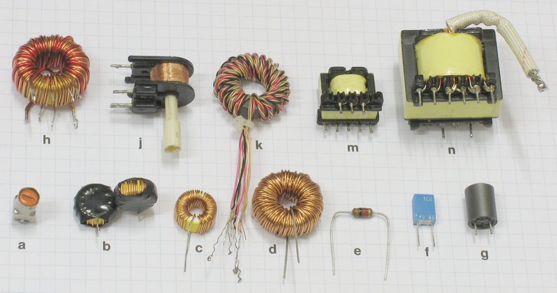 In case you still don't know what you're looking for, I've taken
a picture of some of my junk-box inductors (click picture to open a
larger version in another window).
The grid is 5x5mm, so you can get some idea of size.
In case you still don't know what you're looking for, I've taken
a picture of some of my junk-box inductors (click picture to open a
larger version in another window).
The grid is 5x5mm, so you can get some idea of size.
|
| a. | Variable inductor, as found in FM radios. Okay, it has a ferrite core, but only a very small coil. <1µH, absolutely useless. |
| b. | Two chokes salvaged from a defective PC power supply (AT style), used for mains filtering. Note the yellow painted core. Probably 50µH since two in series gives 100µH behaviour. Useless. |
| c. | Velleman 100L1 choke (they call it "deparasite self"). As with Conrad, only available in some countries. Note the yellow/white core. Specified as 100µH; useful only in quantities of 30 and higher. |
| d. | Velleman 1000L3 choke, also iron-powder core but you have to look very carefully to see that. 1000µH = 1mH. Already useful, but three in series works much better. |
| e. | Also 1mH, but now a small-signal type. Can be used, but expect losses due to the ~100Ω resistance of the very thin wire. Uses standard color code: brown-black-red for 1000 (µH). |
| f. | 10mH small-signal inductor. Quite useful if you have nothing else, but inefficient due to the resistance. Labeled "10K" for 10-kilo-µH. |
| g. | 100mH small-signal type; you don't want to know its resistance. Labeled "104" on the top, meaning the same as standard color code. |
| h. | Transformer with yellow/white iron-powder core from the PC power supply. Useless even with all windings in series. Don't bother salvaging it. |
| j. | Variable inductor probably salvaged from an old TV set. The plastic rod has a ferrite core inside; it can be screwed into and out of the inductor to change the inductance. Can be used since the inductance is ~10mH, but the thin wire causes some resistive losses which makes it less than ideal. |
| k. | Apparently salvaged from some wire-wrap project, however not mine since I don't do wire-wrap. Very nice ferrite core with five separate windings. Just two in series (~50 turns total) is all you need. |
| m. | Transformer salvaged from -again- the same PC power supply. Note the outer square of dark-gray ferrite which seems to be held together by yellow tape (actually, it's glued, so no problem if the tape comes off). This transformer has three windings; the 3-pin side happens to have the highest inductance (~5mH). Very useful, and nicely small. |
| n. | The real work-horse transformer from the PC power supply. It has one primary winding (two pins side) and 10 secondary windings, which all share one common ground (the tube that protrudes from the upper end). The right-hand four pins each connect to two separate windings, and on the PCB both the middle two and right-hand two pins were connected together. Of course, all of this is done to reduce the resistance as much as possible, but it also makes it much harder to increase the inductance by using two or more windings in series. As it is, the primary winding has the highest inductance, again ~5mH, which means it doesn't improve much above the smaller transformer. |
Just one more thing about inductors. If you check out datasheets or design webpages for buck converters, you will mostly see much lower inductance values than the 5mH we're aiming at here. That's because those circuits are usually designed for currents of 1A and higher, and higher currents can be handled with smaller inductance values. That may seem quite counterintuitive, since you may point to the fact that, everything else being equal, maintaining a larger current during the "off" periods requires more stored energy in the inductor and thus a larger inductance value. Indeed, you are partially right. However, the average current value is actually not important; the inductance value only influences how much the current rises during the "on" periods, and falls during the "off" periods, in other words the absolute current ripple as a peak-to-peak value. An inductor that gives a 1mA peak-to-peak current ripple at 20mA average, will also give a 1mA peak-to-peak current ripple at 10A average (well, if the wire didn't melt already...). At high currents, this level of accuracy isn't needed at all, so the current ripple is usually specified as a relative value, for example "30% of the output current". For higher currents, this 30% will also be higher, which means that the inductance value can be lower. On the other hand, handling a quite low current of 20mA requires a quite large inductance value to maintain a low current ripple. It is also worth noting that the inductance value can be reduced if the switching frequency is increased, for example going to 1MHz (50-fold increase) would only need a 100µH inductor. This is done in cellphones etc., where physical size is more important than cost; our low-cost "slow" transistors and even slower LM358 don't leave us much choice in this regard.
Diode
For diode D1, in principle any kind of diode will work. A well-known 1N4148 or 1N4001(-4007) is fine, though both these in parallel will even be a trifle better, since the 1N400x is a bit slow to turn on but has a somewhat lower voltage drop after that. We already discussed that this voltage drop is an important loss factor in the entire circuit, and that Schottky diodes can be used to increase efficiency. There are many types of Schottky diodes and any type will do, though mind the maximum current and voltage ratings. Types such as 1N5819 and 1N5822 are often mentioned; the 1N5822 being the high-current variant with the lowest resistance (and the thickest leads). However, both have a maximum reverse voltage of "only" 40V, so for larger Vleds voltages you need to consider alternatives such as the MBR160 (max. 60V) or even MBR10100 (100V).
It is possible to eliminate all diode loss by converting the lost power to something useful, like light. Indeed, you can replace D1 by a LED and it will light up shortly during the "off" periods. The only problem is that LEDs have particularly low maximum reverse voltages, so this is only useful if Vleds will never exceed 5V.
Capacitor
Going further to the right again in the circuit diagram, we encounter capacitor C3. It is specified as 4.7µF, but 1µF will work too, as will 100µF. Ideally, a bigger capacitor should work "better", namely by reducing the ripple voltage across the LEDs, but that's very hard to measure. And since a 20kHz flicker isn't visible anyway, it doesn't make much sense to put in a large capacitor. The circuit will even work without capacitor, but then the current through the LEDs will be highly pulsating (just like in a situation with C3 present but without L1), which makes the current sensing inaccurate. The chosen value for C3 reduces LED flicker and increases current sensing accuracy, while still not taking up too much board space. But if you don't have this specific value handy, any larger capacitance will do.
While you might be afraid that a large capacitor would introduce some delay when reducing the brightness level (Vref), it turns out that this is hardly an issue since the feedback loop will just temporarily switch the PWM fully off until the current has reached its desired value. The same mechanism also makes sure that increasing the brightness is as fast as possible. A slight delay only becomes noticable when using a very large capacitor, say >100µF.
When choosing a capacitor, taking note of the internal resistance (ESR) can be useful but won't matter very much. The maximum voltage is of much greater importance. At times, C3 will see the entire Vleds voltage (for example when you change LEDs), so it must be able to handle that. Since a capacitor at its rated maximum voltage has a guaranteed lifetime of only 1000 hours, you'd better overdesign this aspect by a factor of at least 1.5 to 2. The same holds for C2, C5 and C6.
LEDs
There can be any color, any size and any number of LEDs, as long as their total forward voltage doesn't exceed Vleds (else they can't be turned on fully), and as long as they are "normal" LEDs that need 20mA current to turn on. This LED dimmer, as drawn, is not suitable to drive the 1W or 3W Luxeon Power LEDs or similar types, though it would of course be possible to adjust the design to handle the 350+mA currents required for that.
Current sense and compare
The current through the LEDs is sensed by R7. Any resistance value will do, given that R13 is calibrated properly, but lower values are better since the amount of power lost by R7 is proportional to its resistance. A 1Ω resistor is about the smallest that will operate reliably, though any value in that neighborhood will work just as well.
As discussed, the gain of IC1b is somewhat limited by R8 and R10. Their values aren't very critical, but the resulting gain shouldn't be much lower than as drawn. Only if you choose R7 "very" high, say 10Ω or near that, it makes sense to reduce the gain somewhat by setting R8 to 470Ω.
We already discussed R9 and its value above.
The PWM control voltage is smoothed by R11 and C5. Exact values are not important, as long as the RC-time is much longer than 1/20000=0.00005 while still being short enough to be unnoticable when adjusting the brightness level.
Reference voltage generation
Apart from T3, T4 and R12, everything in the reference voltage circuit depends on the value of the potentiometer R15. Easy things first: T3 and T4 can be any kind of PNP transistor, even different types, yet preferably with nicely high current gains (>100). R12 needs to supply the base current for T4, for which less than 1/100th of its already tiny collector current already suffices, so any value <1MΩ will do.
The idea is that you can salvage basically any potentiometer from some defective device like a portable radio or a CDROM drive, since that's usually cheaper than buying new and, even when buying new, you don't always know what to expect. That's why the circuit will work with any pot in the range of roughly 500Ω to 50kΩ. That lower boundary is only to keep the required current nicely low (<0.1mA); the high boundary is mostly determined by R16 which can't go much higher than 100kΩ. The shown value of 10kΩ for R15 is just because that value happens to occur frequently. If you have a stereo pot, it makes sense to connect both tracks and wipers in parallel, since that reduces the chance of complete "unconnectedness" of the leads. A logarithmic pot is fine (instead of a linear one), but you'll find that one way of connecting it provides a much smoother brightness control than when the connections are reversed. This of course has consequences for the pot orientation when placing the circuit in some enclosure.
As discussed above, R14 should be chosen (nearly) equal to R15, to have a maximum LED current of 40mA in cases where the bottom lead of R15 doesn't make contact. R14 may also be chosen smaller; indeed, when R15 is greater than 10kΩ, it wont hurt to keep R14 at 10kΩ anyway.
With all other components chosen, the maximum brightness (maximum LED current) is determined by R13. We can derive a formula to get a basic idea for the value of R13, as follows. Let Imax be the desired maximum LED current. Then the maximum voltage across R7 is given by V7 = R7*Imax, but this is also the maximum reference voltage. (We ignore the effect of R8 and R10 here.) This voltage should occur when R15 is at its maximum setting, so V7 is also across R14, R15 and R16. Then the total current through these resistors, which is the collector current of T4, will be Ic4 = V7/R14 + V7/R15 + V7/R16. That same current (plus a trifle due to the base current of T4, minus a trifle due to the base current of T3) will flow through R13, which should be chosen so that this exact current will produce the approx. 0.68V emitter-base voltage of T3, in other words R13 = 0.68/Ic4. Substituting and mangling gives:
R13 = 0.68 / (R7 * Imax * (1/R14 + 1/R15 + 1/R16))
or, if you prefer:
R13 = 0.68 * R14 * R15 * R16 /
R7 * Imax * (R14 * R15 + R14 * R16 + R15 * R16)
With the values for R7 and R14-R16 as shown, this gives a first estimate for R13 as 162kΩ, so either 150kΩ or 180kΩ when selecting from the E12 series. However, it turns out that this value is a bit too high (and the current and Vref a bit too low), due to some simplistic assumptions we made, and a value of 120kΩ turns out to produce a maximum LED current of almost precisely 20mA. The easiest way to determine what works best in your case is to simply try various values, starting with the calculated first estimate, and just measure the LED current with your multimeter. You can short out one of the LEDs with the multimeter leads if you find that easiest; just do not short out all LEDs, since that would require the buck converter to generate a very low voltage (<0.1V) over the multimeter and R7, and the current can not be maintained very accurately when doing that.
The current as determined by R13 varies slightly with the supply voltage, so that also holds for the maximum LED brightness. Usually that shouldn't be a problem, but in case you happen to be extremely cautious, you should "calibrate" R13 at the maximum expected supply voltage to produce a LED current slightly below 20mA. On the other hand, if you like pushing your luck and driving the LEDs way past their maximum rated current (say, at 40-45mA like some LED flashlights like to do), that's possible as well. Just remember that R6 then also needs some adjustment, at least when Vleds < 10V.
Supply voltage / batteries
When driving the circuit from one or more batteries, pay attention to the expected voltage level in relation to the number of LEDs you want to use. "Primary", non-rechargeable batteries like zink-carbon or alkaline exhibit a roughly linearly decreasing voltage level, starting at 1.5V per cell when fresh, and ending at approx. 1.0V per cell at the end of their lives. So to be able to use the LEDs at maximum brightness for the entire battery life, make sure that the total LED voltage can still be delivered when each cell produces only 1.0V. And do measure the LED voltage, since it may vary quite widely between types and manufacturers (there are both 3.1V and 3.8V white LEDs).
Rechargeable batteries (Ni-Cd and Ni-MH) will deliver voltages higher than roughly 1.15V until nearly completely discharged, so it is safe to take that voltage as a guideline when comparing to the total LED voltage. An additional issue is that these batteries shouldn't be discharged under 1.0V per cell. This means that it makes sense to always use the maximum number of LEDs possible, so that the LEDs stop burning before any deep discharge occurs.
When considering the attractive option of using the small 9V "radio" batteries, note that "primary" types always pack 6 cells, so the supply voltage can be expected to decrease almost linearly from 9V to approx. 6V at end of life. This means that two white LEDs is the maximum, and even then some dimming can be expected when the battery is nearly empty. Rechargeable "9V" batteries pack either 6, or 7, or 8 cells, depending on the manufacturer and the price point. More cells may mean less capacity per cell, but not necessarily. Anyway, the voltage is never exactly 9.0V, so some manufacturers only say "for 9V applications". Two white LEDs is still the maximum, unless combining a good 8-cell battery with relatively low-voltage white LEDs.
Note that rechargeable batteries do not have very long "shelf lives". Do not expect a rechargeable battery to function at all after having laid untouched for more than a year. Either discharge-recharge them every 6 months or so, or leave them tricke charging continuously (Ni-Cd only). Panasonic offers a number of PDF documents on all kinds of batteries and their charging methods.
The circuit does not include protection against reverse voltages, which may readily occur when trying to connect a 9V battery the wrong way and the device is switched on. For efficiency reasons, it is not advisable to include a diode in the supply line, but it is still possible to add a reverse biased diode over the entire supply voltage. Combined with a relatively high rated fuse (100-200mA) before the diode, it should make sure that the fuse burns immediately when a reverse voltage is applied, while the rest of the circuit only sees a 0.7V negative voltage for a few milliseconds.
To end this section, some quick words about the "battery helper" capacitors C2 and C6. Larger capacitances are always nice, but not very useful. Do mind the maximum voltage ratings, and keep them at least a factor 1.5 to 2 above the maximum expected supply voltage levels.
Circuit modifications and other uses
The circuit as drawn may not be directly useful for your purposes. In this section, we'll briefly examine a few straightforward modifications to the circuit to help you get going.
More LEDs
The buck circuit can only produce voltages lower than Vleds. When using a nice and small 9V battery, that means you can only drive two (2) white LEDs of 3.2-3.5V each. While two LEDs produce quite much light already, it's only natural that You Want More. There are several options available.
1. Use a higher supply voltage, for example three or four 9V batteries.
Note that the supply current of the LM358 is basically independent of the supply
voltage, so it makes very much sense to keep Vlogic at 9V and use
the extra batteries only to increase Vleds. At higher voltages, you'll
want to increase R6 to keep the power loss small, see above.
When going higher than 40V (Vleds only!), these are the components
that you need to change: T1, T2, D1, C2, C3 and R6.
Again, see above.
2. Build two or more separate circuits.
You can have a separate reference voltage for each of them, which would
for example enable you to create any color from the combination of
three separate circuits driving red, green and blue LEDs respectively.
On the other hand, IC1b hardly loads Vref at all, so it is very well
possible to have just one reference voltage which controls all circuits
at once. In such situations, the effect of IC1b's offset voltage
and its compensation by R9 is easily visible, since it requires quite
some experimentation with different R9 values to have all LED strings
turn on at exactly the same dimmer setting. However, at full brightness
this difference between the separate circuits will be completely unnoticable,
so you probably shouldn't invest too much time in perfecting the lower end.
As already mentioned above, having multiple separate circuits allows you to
efficiently combine IC1a-s and IC1b-s of separate circuits and choose
different types for them to match their different functions.
In case you want to be able to switch circuits completely on and off
separately, and you have not combined IC1a/b with
other circuits, it suffices to switch off Vlogic only (i.e. the IC1
supply line), since the
remaining current through Vleds will be less than 0.02mA. And when
using a single Vref in such a separate-on/off situation,
it could make sense, depending on your circuit layout, to drive the
reference voltage generation from Vleds instead of Vlogic, in order
to keep it working at all times.
3. Parallel LED strings in one circuit.
As some LED-driver datasheets suggest, it is possible to have the buck
converter drive multiple D2+R7 strings in parallel, while only sensing
the current of one string. When the LEDs in the separate strings are
exactly matched, they will draw the same current at the same voltage
level, and be equally bright. Yet since this is very hard
to realize, it is wise to increase the R7s to 10Ω
so that they will handle the voltage differences (then also increase R8
to 470Ω and adjust R13 to match).
Of course this only works with exactly the same number
of LEDs in all strings, the same color, from the same manufacturer and
actually from the same manufacturing batch. (This in contrast to the
multiple-circuit solution above, which allows fully arbitrary mixing
of LEDs.)
To determine which LEDs are perfectly equal, you can build
a current source like circuit (b) far above, and having it drive two
LEDs in parallel. If they both light up at half brightness, they are
perfectly matched. But usually you will see that only one LED lights
up fully while the other one remains dark; the former then has a
slightly lower voltage drop than the latter. This way, it is easily
possible to sort your entire LED collection on the forward voltage
drop, which also allows you to readily select pairs of LEDs
that perfectly match other pairs of LEDs, even while the
individual LEDs may differ quite much from one another.
When driving multiple strings of LEDs at once, the current through T2
will increase accordingly. This probably means that you need a lower
value for R6, and possibly a "fatter" T2.
4. Boost circuit.
While a buck converter can only produce voltages lower than
the supply voltage, there are other Swich-Mode Power Supply topologies
which do not have that limitation. The easiest is the boost converter,
and again
Google
knows where to get more information. The LED dimmer can be
redesigned to have a boost circuit, however note that a large and
low-resistance inductor and also a large capacitor are of paramount
importance in a boost circuit. You may be tempted to drive a boost circuit
directly with T1, but that is not wise since the slowness of IC1a
makes T1 operate in linear mode very often. For the highest efficiency,
a second stage remains necessary; you may opt to keep operating the "new" NPN
T2 inverted with respect to IC1a, and switch the positive and negative inputs
of IC1b to keep the regulation working properly (though mind the gain).
Further, do note that a boost converter's output voltage is
minimally equal to Vleds, so make sure that your LED string is
completely off when connected to Vleds, otherwise you'll never
be able to obtain 0% dimming. And at the other end, duty cycles >~80%
may result in a collapsing output voltage, which determines the
maximum output voltage that the boost ciruit is able to generate
(usually 3-5 times the input voltage). Going beyond this maximum
will probably result in IC1b increasing the duty cycle even more, which
will have the opposite effect and immediately create a short-circuit
at 100% duty cycle. This will also happen automatically whenever
the LED chain comes loose, because IC1b will try to increase the voltage
far beyond the maximum in a desparate attempt to maintain the desired LED
current anyway.
In extreme cases, it might turn out to be necessary to set the
dimming back to 0% and switch the circuit completely off and on again,
in order to restore it to proper operation (if the components haven't
burned down already). In other words: be sure to add a fuse of some
appropriately low current rating, and expect it to blow every once
in a while. Of course, this all is mainly caused by us wanting to control
the current of the LEDs. For voltage-controlled boost
converters, this risk doesn't exist, since the control loop will
set the duty cycle back to near-0% when no load is attached.
If you happen to have a ferrite-core transformer handy anyway,
it is possible to overcome the lower limit on the number of LEDs
as posed by the boost circuit, namely by changing the design to a
Flyback
converter. Yet this design still has the same problems at 100%
duty cycle.
In both the boost and flyback circuits, the switching transistor needs to
handle large currents, and in the flyback circuit also high voltages.
The advantage of both circuits is that the switching transistor (NPN type)
can be driven from Vlogic instead of Vleds, which may reduce the power loss
somewhat even when a low-gain transistor needs to be applied.
5. Add a charge pump
To overcome the mentioned problems associated with using an inductor to
obtain a high voltage, it is possible to use a capacitor-only
circuit with an inherently well-defined maximum output voltage: the
charge
pump. Connect the output of the charge pump to Vleds; mind the
voltage ratings of all components involved.
Of course, this means that the energy is passed through two complete
circuits before it reaches the LEDs.
Even so, the high efficiency obtainable by a well-designed charge pump
combined with the high efficiency of
the buck circuit (especially when operating at 80-100% duty cycle)
may very well give a slightly better result than using a
boost or flyback converter to do both the voltage-increase and
current-control jobs at once.
I found an interesting
charge
pump circuit
on geofex.com which does not require an inverted drive line.
As far as I can see, there is no reason why it couldn't be driven
from just about any oscillator with a decent high-current output, like
the well-known NE555. (Mind the 16-18V maximum supply voltage,
and note that its CMOS cousin ICM7555/LMC555/TLC555
has greatly reduced current sourcing capabilities.)
Ideally, the charge pump should operate at a much higher frequency
than the buck circuit to allow for optimal power exchange during the
buck's "on" periods. With the buck circuit operating at approx. 20kHz,
the charge pump should be designed for at least 60-80kHz.
The duty cycle of the charge pump should probably be near 50%;
the LM555 datasheet gives a simple circuit to achieve that
without using the output pin.
Only, you will probably notice that an NE555-driven charge pump is
mainly useful for demonstration purposes only, since its relatively high
supply current drain and relatively low high-output voltage mean
that the total efficiency can't be very high.
So, if you want to use an efficient charge pump for any practical purpose,
you'll have to look a bit further still.
Voltage control
Instead of controlling the current, you may want to control the voltage across the load. Of course, this is quite unsuitable for LEDs because of their weird voltage-brightness relation, but indeed, there are many loads that require a stable voltage regardless of the current they draw.
Converting to voltage control is as easy as removing R7 and connecting R8 to a voltage divider parallel to C3. Maintaining proper operation of the gain limiting feedback loop will probably mean that the total resistance of the voltage divider can't be higher than, say, 50kΩ. You probably won't need R9 in this case, since the offset voltage of IC1b is negligable when compared to the tolerance of the voltage divider's resistors.
If you want an adjustable voltage, the Vref generation circuit can still be used, though the best results can probably be obtained by using a (much) wider voltage range, such as 0 to 1V instead of 0 to 0.020V. Unlike the current controlled version, which needed very low control voltages in order to keep power losses due to R7 as small as possible, this is no concern in a voltage controlled version, since the voltage divider's power loss only depends on its total resistance and not on the relative "height" of the sense point. (Indeed, it would even be possible to sense the output voltage directly, only then we'd soon bump into the upper input voltage limit of IC1b, which is specified as Vlogic minus 1.5V.)
On the other hand, if you want one specific output voltage, and want it to be maintained very precisely independent of Vlogic, your best option is to use a simple two- or three-terminal "micropower voltage reference" and connect it directly to the positive input of IC1b. You can then design the sense point of the voltage divider to produce the reference voltage exactly at the desired output voltage. Using a potentiometer will allow you to fine-tune the output voltage, or... make the output voltage adjustable again.
Note that, depending on the load, it will usually be highly advisable to use a very large capacitor for C3, larger than 100µF or even larger than 1000µF. And again, the circuit as drawn is suitable mostly for loads that draw average currents up to 20mA; you can change R6 and/or T2 to accomodate your specific situation.
If you need to drive large currents at a constant voltage, you might want to investigate integrated solutions like the LM2574-79 series of switching regulators. For example the LM2576-xV 3A buck regulator and LM2577-xV boost/flyback regulator series basically only require an external L1 (mind its current rating), C3 and D1. But since they all draw 5-10mA supply current, they only become interesting (i.e. efficient) for relatively high-current loads, say 100mA or more.
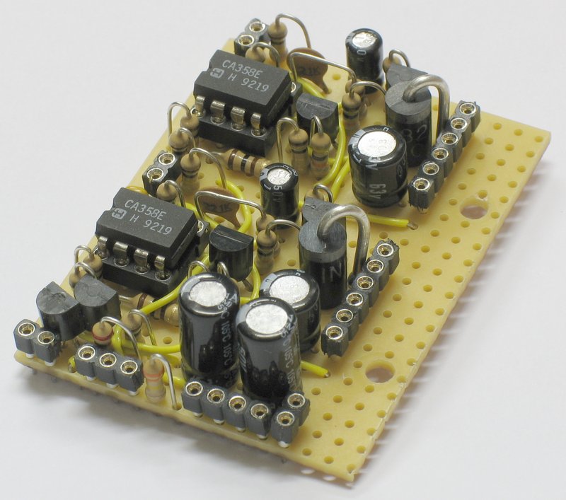
Building
At first, you probably want to build the circuit on a solderless breadboard, in order to find the most suitable component values for your situation. The circuit is small enough to fit on the smallest breadboards available (the ~250 contacts types). Don't try to push in the 1N5822 though, as its leads are just too thick; soldering some thinner wires onto them will help a lot. Of course, the same holds for R15 and possibly L1.
The procedure for "calibrating" the component values is roughly as follows:
- Start with your "biggest" L1; R6 at 10kΩ (or as low as 1kΩ when using a low-gain T2); no R9; and R13 as calculated by the formula above. You should be able to control the LED brightness over a fairly wide range, for any number of LEDs and any supply voltage. If not, back to the drawing board.
- If you can't turn the LEDs fully off even with R15 turned fully down, you need offset voltage compensation by means of R9. So try different values for R9, starting at 1MΩ, and settle for the highest value that still gives full dimming ability. Since the offset compensation by means of R9 varies with the supply voltage, you'll want to find a suitable R9 value at the lowest expected Vlogic voltage. Also, remember that a different compensation will be required for each and any LM358 you'll encounter.
- With the lower end sorted out, now try different values for R13 to make sure the high end works well. To get the longest lifetime out of your LEDs, make sure the current through them doesn't exceed 20mA even at the highest supply voltages. As already discussed, it's okay to short-circuit one LED with your mA-meter, as long as at least one LED remains operational.
- Next, insert your mA-meter in the Vleds supply line, and use "enough" LEDs (at full 20mA brightness) to get "approx." 10mA supply current on Vleds. Then try all inductors you can find, and stick with the one that results in the lowest supply current. In case you're winding your own inductor, keep adding turns in batches of 10, until you notice no further improvement.
- Then try variants for R6, both lower and higher values, to obtain the best compromise between T2's switching speed and the base current power loss due to R6.
- Finally, check if your R13 value is still appropriate; you'll probably find that it is, except when you started with a "totally wrong" guess for L1.
After building on a breadboard, you might just want to make a more permanent version. Personally, I don't bother making a custom PCB for circuits like these, as I find generic 3-holes-per-pad "prototyping" PCBs just as handy. In some countries it's called a TriPad board, and in case you aren't familiar with it, it's just stripboard (aka Veroboard) with the strips pre-cut after every three holes. It holds a very comfortable middle ground between the work required to cut a "full-strip" board and the work required to manually form tracks on perfboard (or 1-hole-per-pad), while still allowing very tight circuits to be built with sufficient forethought. It's available from for example Maplin with product code JP52G, or from Velleman with product code ECS3 (often sold without the Velleman brand name, but with the correct product code).
 That said, nobody forces you to use anything, and you should feel
free to use whatever you're comfortable with.
It's just that I have made a nice circuit layout for the TriPad
board, that you might find interesting.
Click on it to open the printable
PDF version;
also available in
PostScript.
You can edit the original
Xfig file
if you want a different layout,
using
Xfig,
also on
Windows.
(Note: GNU GPL ≥2, so if you publish anything based on
these files, you must also publish your own source files.)
That said, nobody forces you to use anything, and you should feel
free to use whatever you're comfortable with.
It's just that I have made a nice circuit layout for the TriPad
board, that you might find interesting.
Click on it to open the printable
PDF version;
also available in
PostScript.
You can edit the original
Xfig file
if you want a different layout,
using
Xfig,
also on
Windows.
(Note: GNU GPL ≥2, so if you publish anything based on
these files, you must also publish your own source files.)
This layout works for TriPad boards, but should also work on stripboard when you carefully cut the tracks at the right places (no need for wire 7 then), and on perfboard when you carefully bend the leads of every component to create the correct tracks.
The circuit layout could use some more explanation. First of all, you'll notice that the layout consists of two parts, namely one for the reference voltage generation and one for the actual buck circuit, much like in the schematic diagram far above. This is to accomodate re-use of the reference voltage by multiple circuits. With some closer inspection, you'll notice that the layout is perfectly stackable, which means that (in this case) the Vleds and gnd strips ("rails") continue all the way from the top to the bottom. The empty space between both "modules" is of course only for clarity, and can be ignored in practice. Note that C2 is included in the "control module" for space reasons; be sure to add additional C2s when driving more than 2 circuits at once, each C2 close to its own circuit.
Solid lines pertain to the upper side of the PCB, dashed lines to the underside (solder side). The quartered circles indicate possible positions for screws; either on the right-hand or left-hand side, or maybe even both. The component placements should be quite clear; their leads should go in the holes that the solid lines end in. And whenever a component's lead continues in a dashed line, bend the lead in that direction and solder it also to the adjecent solder pad. Besides the various components, the layout has ten (sets of) wires, sometimes also named wire bridges or jumpers, numbered from 0 to 9.
Red lines warrant early attention, namely wire 0 that needs to be placed together with R18 and before C2 and C6, and D1's holes that should probably be enlarged before anything else. Indeed, two leads in one hole will work (otherwise enlarge the hole a bit), and that is also required for wire 9 (Vref) and R9-R10.
Gold (or brown) means alternative or optional: C3 and C5 can be shifted to accomodate various physical shapes (e.g. radial/axial); wire 5 can go under IC1's socket if possible; and R9 is an optional beast that (when needed) should go in together with R10 and after wires 3 and 9. Okay, I confess, I made the layout for my LM358s that do not require R9, that's why R9 is in such a weird place.
Green indicates a connector, though it's perfectly okay if you solder everything to the board directly. Only I made this layout specifically to be suitable for some further experimentation, and having things removable is quite handy then. I particularly like single-row "machine tooled low profile IC sockets", or "collet sockets", since they provide breadboard-like functionality at a very agreeable price point. At the lower right-hand corner, you could combine a 5-pin and 1-pin socket, but using 4-pin and 2-pin instead will give much greater stability. Vlogic is drawn as a connector to either allow it to be switched on and off independently, or to route it to other circuits.
Almost everything is mounted vertically (i.e. using the smallest board space), with the single exception of R8; and R9 is a special case. C4 is a multi-layer ceramic capacitor, basically a tiny SMD version with leads attached. Also see the photos below.
When soldering components, I generally prefer to work from the lowest
profile components up to the highest profile ones; this allows me to
keep all components easily accessible. The wires are last, so they
can be routed around components. If you don't know where to start,
you can take this as some guidance:
enlarge holes for D1;
solder IC1's socket;
the "green" sockets if you want them;
ceramic caps C1, C4;
R8;
all transistors;
R16 with wire 0;
R2, R3;
R5, R6, R11, R14;
R4, R7;
R12, R13 if not in socket;
R1 (note the special "bridge" construction);
C3, C5;
D1;
wire 2 (A0 to either A1 or A2);
C2, C6;
wire 1 and 3-9;
R10, plus R9 if required;
Vlogic connections when using no sockets.
My usual soldering iron had a hard time heating up the 1N5822's massive
leads, so I cheated and pre-heated the leads with a high-wattage
soldering gun. The leads stay very hot for a long time; mind your
fingers.
Pictures
To give you some further inspiration on how to build the circuit and how to use it, here are some pictures of the construction of my working prototype dimmable LED flashlight. Click on a picture to open a larger version in another window.
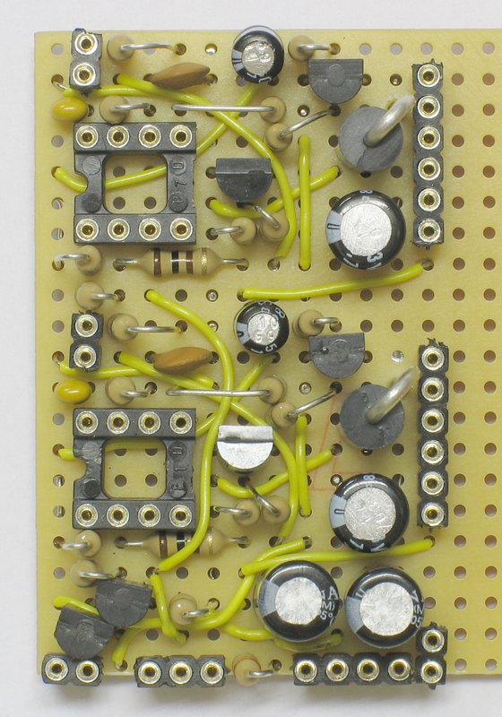 |
The circuit mostly finished. Actually, there are two "real" buck circuits, controlled by one reference voltage. Note that wire 5 could be routed under these particular IC sockets. R14 is still absent, because I didn't yet decide which potentiometer to use for R15. |
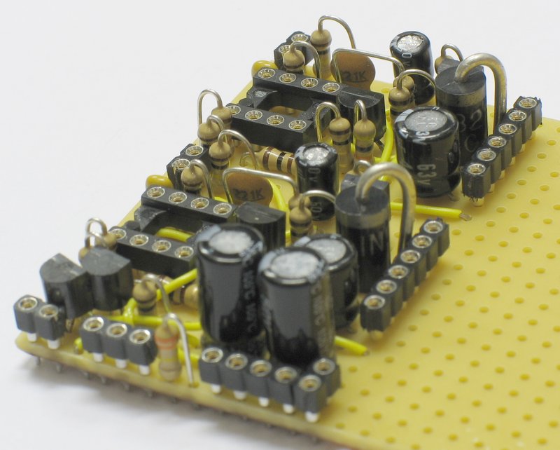 |
Note the very thick leads of the 1N5822. The "bridge" construction of R1 should become clear from this angle; the same holds for the "green" sockets in case you didn't understand yet. |
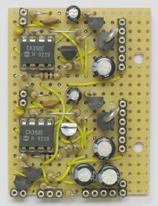 |
The complete circuit including IC1-s. R14 added as 22kΩ, to accompany a 50kΩ stereo potentiometer with tracks wired in parallel. |
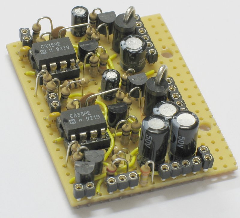 |
And a different angle shows some more details. |
| A side view shows that D1 is the highest-profile component, followed by C2 and C6. |
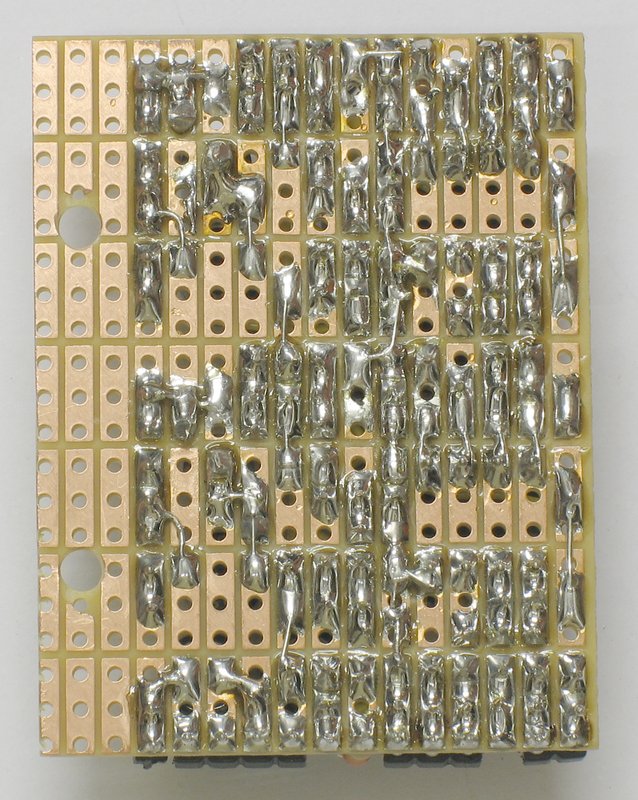 |
A look at the solder side makes clear what is meant by the dashed
lines in the layout drawing.
Note that this is the authoritative circuit version; if you happen to notice any difference with respect to the schematic diagram or the layout drawing, then the latter are wrong. |
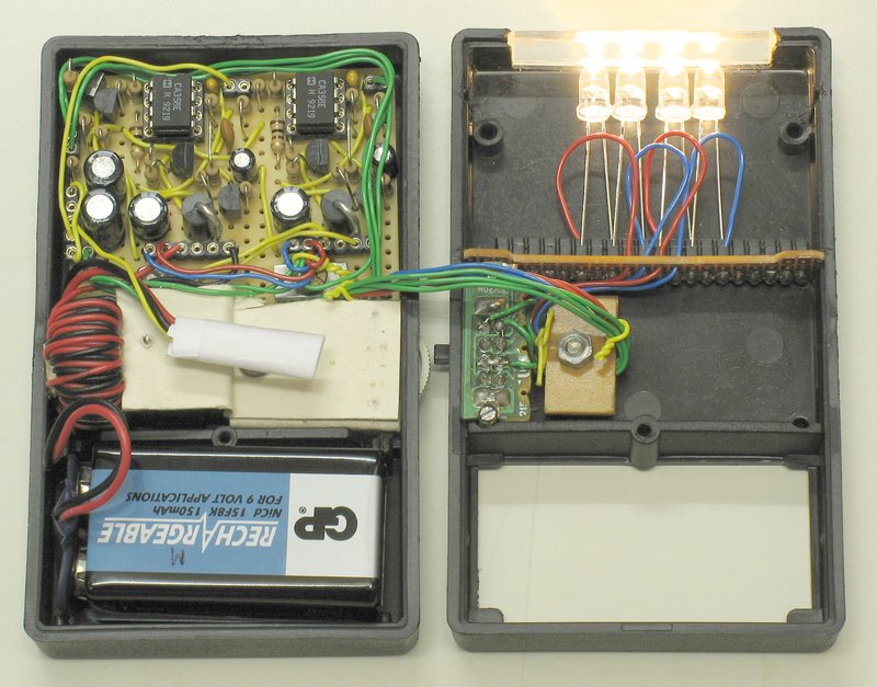 |
The complete circuit mounted in a tightly fitting box that I bought years ago during some sale. Interesting things to note are the wires that go in the sockets, the red-black wire which is one of the inductors (ferrite core, salvaged from yet again the same PC power supply), the 9V battery in its very own compartment, the hidden potentiometer (salvaged from a defective CDROM drive), the off-on1-on2 switch with attached PCB, and the LED assembly. The paper-wrapping just houses a semi-permanent coupling of the flexible 9V connector wires to the (thin) solid wires that go into the sockets. |
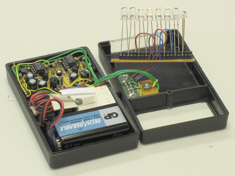 |
The LED assembly slides into the box, and also out of it, which makes it easy to change the LEDs. Since the construction has space for more LEDs than the circuit can drive, it allows one to carry spare LEDs... |
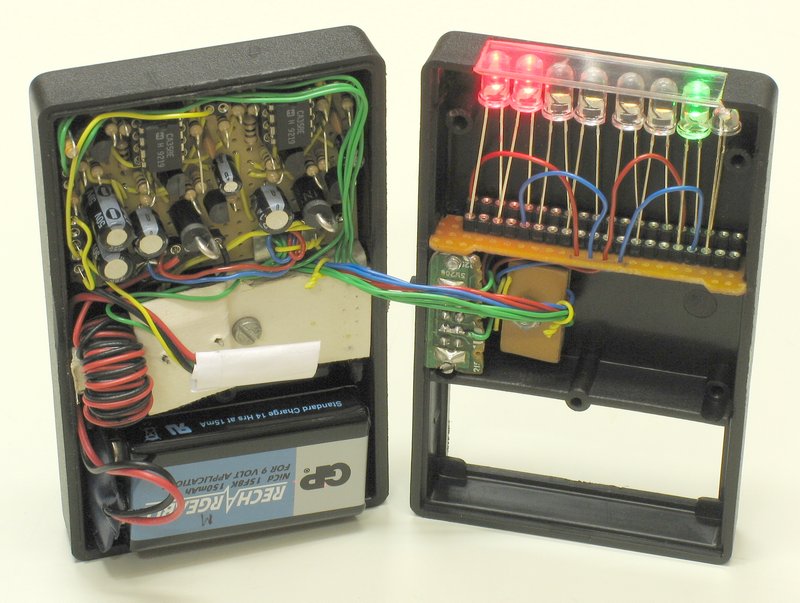 |
...or LEDs in a variety of colors to suit any occasion by simply rewiring.
In this view, it's also clear that the LED assembly is built out of my favorite IC-type sockets. Since this project isn't meant to commit itself to any specific LEDs, cutting their leads is no option, which means that both, different-length leads need to be accounted for. It was possible to raise the furthest socket row slightly by not soldering it tightly to the board. The nearest row was lowered by enlarging the PCB's holes so that the thick metal part below the black plastic could fit in completely. The sockets are interconnected "vertically", each "high" hole to the nearest "low" hole, much like a mini breadboard. If you build this on perfboard, do not bend the "low" socket's leads sharply to connect to the "high" socket's leads, since the leads will break very easily. Instead, bend them carefully in an upside-down "U"-like shape. As long as the angle is gentle everywhere, it will hold just fine. Next to the red-black-wire coil, this photo also shows the leads of the second inductor, which is a PCB-mounted type salvaged from the electronic ballast inside a defective screw-in fluorescent lamp. It resembles type "m" from the inductors photo above; just a bit smaller and with only one winding. |
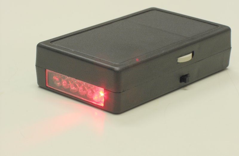 |
This photo, and the next one, show a LED configuration that could be useful for people working in the dark, like astronomers. The "stereo" three position slide switch, which I salvaged from an old VCR, selects either full-off, 1-circuit-on, or 2-circuits-on. In other words, you can have both dimmable night vision preserving red light... |
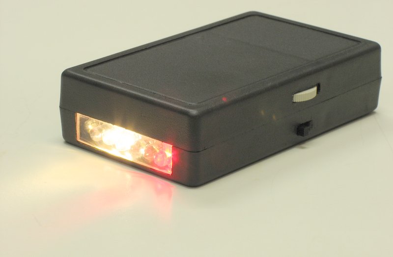 |
...and dimmable high-CRI warm-white light (+red) from the same flashlight.
From earlier photos you can probably determine how this is accomplished. The battery's positive terminal is wired to both of the switch's central contacts, and the position '0' contacts are unconnected. Vlogic of circuit 1, and Vleds, are wired to both positions '1' and '2' of the "right channel". And Vlogic of circuit 2 is wired to only position '2' of the "left channel". On the PCB, the reference voltage circuit is driven from Vleds ["A0" to "(A1)"], so it's on whenever needed. Of course, since there is only one reference voltage, both LED strings are always driven at the same current. |
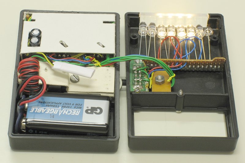 |
To reduce the risk of a short-circuit, and also to make the flashlight
look more elegant when peeking in from the outside,
I prepared a piece of cardboard to cover most of the circuit.
To preserve as much space as possible for the LEDs,
I opted to cut holes in the cardboard to accommodate the highest profile
components. This includes the socket-mounted R13 in the upper left corner.
By the way, this probably is a polypropylene ("PP") box, demonstrated by the fact that I couldn't glue anything to it. The nice thing is that PP will readily melt, so I could just gently push in some flat-head screws and nuts while heating them with a soldering gun. This works best when the contact area is as large as possible, so I sawed some fairly deep ridges in the metal parts before melting them into the box material. Since the walls of the box are very think (>2mm), it was possible to sink the parts quite deep into the box material without causing any deformation on the outside. |
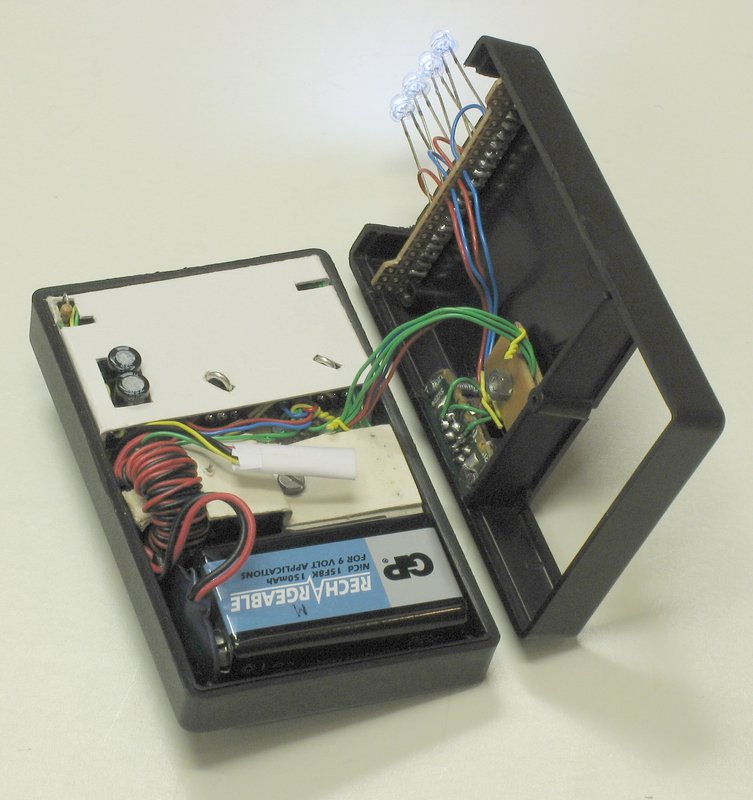 |
From the previous picture, you might wonder about the purpose of the horizontal holes at the far end of the cardboard. These are needed when the LED assembly is used in its alternative position, which is almost at the top of the box. This position can be used to easily change LEDs without opening the box... |
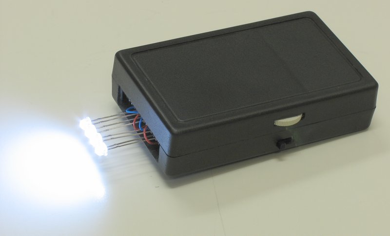 |
...but is actually required to make optimal use of broad-angle LEDs like these 120° blue-white types. To accomodate this, the transparent window (made out of a relatively thick cassette tape box) can also slide in and out. |
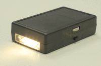 |
And to conclude, a little animation showing 0-100% dimming in both 1-circuit and 2-circuits mode. If you watch closely, you can see the switch alternate between positions '1' and '2'. |
In case you're wondering where to get the box pictured in the photos above, it's not available anymore. For reference, the outside dimensions are 101 x 60 x 25mm, with a 9V battery compartment. You can take this as absolute minimum dimensions for a 2-circuit design. Similar, slightly larger boxes are available as Conrad part# 522473 or 540889, Velleman products G3011, G939 or G407, or Nedis type "BOX KM33B" (always sold without the Nedis brand).
But, if you happen to have an unused super-low-cost plastic 2 D-cell flashlight lying around, the battery component should provide just enough space to hold a 1-circuit PCB and one 9V battery. Or, if you make a super small double-sided custom PCB with SMD components, you might even be able to fit in two 9V batteries -- and twice the number of LEDs. In either case, it's probably easiest working with a cardboard tube that slides into the battery compartment, rather than fixing things directly to the plastic (or whatever).
Measuring
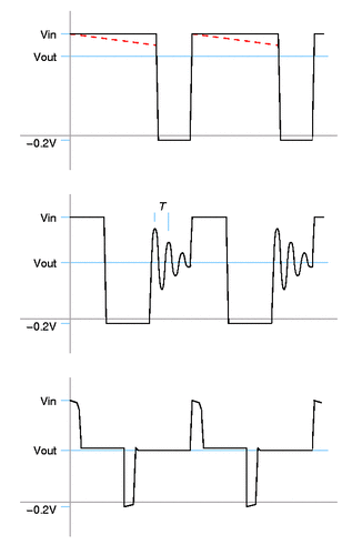 A simple multimeter is enough to determine that the LED dimmer works
properly, and also that it works optimally (given your situation).
This makes it an ideal project for electronics enthousiasts that don't
have access to expensive measuring equipment.
But if you happen to have an oscilloscope
handy anyway, you can use it to gain some more insight into the inner
workings of the circuit. While you could of course examine any and all
voltages and components, the voltage across D1 tells more about the
circuit than any other. To the right, three scope traces are
sketched that you may encounter across D1 in various situations.
(Sketched, meaning that some artistic liberty was taken to
make things easier to understand.) The black line is the voltage
across D1; Vin and Vout refer to the buck circuit's input and output
voltages, so Vin is Vleds, and Vout is the voltage across C3 (and
D2+R7).
A simple multimeter is enough to determine that the LED dimmer works
properly, and also that it works optimally (given your situation).
This makes it an ideal project for electronics enthousiasts that don't
have access to expensive measuring equipment.
But if you happen to have an oscilloscope
handy anyway, you can use it to gain some more insight into the inner
workings of the circuit. While you could of course examine any and all
voltages and components, the voltage across D1 tells more about the
circuit than any other. To the right, three scope traces are
sketched that you may encounter across D1 in various situations.
(Sketched, meaning that some artistic liberty was taken to
make things easier to understand.) The black line is the voltage
across D1; Vin and Vout refer to the buck circuit's input and output
voltages, so Vin is Vleds, and Vout is the voltage across C3 (and
D2+R7).
The top trace is what you should see when the circuit operates near maximum brightness. During the relatively long "on" times, L1 is fed with Vin, which causes the current through L1 to ramp up. D1 is reverse biased and does not conduct; in other words: it is effectively removed from the circuit. During the following "off" period, L1 "discharges" itself via the LEDs, R7 and D1. This makes D1 be forward biased, which means it shows a nearly constant voltage of 0.2 to 0.3V (assuming a Schottky diode). The current through D1 flows bottom-up, so we measure this as a negative voltage. Before the current through L1 is fully "discharged", another "on" period follows, and everything is repeated.
During the "on" periods, the current through L1 ramps up, and that current is delivered via T2. If you see the voltage across D1 ramp down during the "on" periods, as indicated by the dashed red line, it means that T2 presents itself with a large resistive component. This can happen when T2 is not driven far enough into saturation (decrease R6) or when T2 just isn't capable of transporting the required current (only applicable for total load currents >100mA; choose another T2 then).
The middle trace is what you get when you turn the brightness down. L1 isn't able to store enough energy during the "on" perionds, so it can drive the LEDs only during the first part of the "off" periods. After that, L1 starts enjoying itself while leaving C3 to do the hard work. This is called discontinuous mode, meaning that there are times that L1 doesn't contribute to the output current. Ideally, you'd then expect L1 to behave just like any wire, and D1 to behave as if not present, so you'd expect the trace to be (nearly) flat at the Vout level. But instead, it starts resonating around the Vout level (though it may be much less than shown here). This is not caused by your measuring equipment, but is a direct consequence of the L1-D1-C3 combination. At the moment that L1 has completely emptied itself, it sees a voltage of Vout at its right side thanks to C3, and 0V at its left side because D1 just stopped conducting. So a current starts to flow through L1 in the reverse direction, to charge D1 (which behaves like a tiny capacitor in reverse bias) up to the Vout level. But, being an inductor, L1 doesn't quite know when to stop, resulting in an "overcharged" D1, followed by a "forward" current to empty it again, but too far empty, etcetera. Classic LC resonance.
[In case you choose not to believe me, feel free to do your own experiments. You will notice the following regarding the resonance frequency: it will not change for different values of C3; it will increase when L1 value is decreased by adding an inductor parallel to it; it will decrease when D1 capacitance is increased by adding a smallish capacitor (approx. 1nF) parallel to it; it will not change when decreasing the scope capacitance by measuring via a small capacitor; and it will decrease when the number of LEDs is decreased, since the reverse bias capacitance of a diode increases at lower reverse voltages.]
When you look up D1's (voltage-dependent) reverse-bias capacitance in its datasheet, and determine the time constant T from the scope trace, you can get a rough idea of the inductance value of your coil. The LC-resonance formula f = 1/T = 1 / 2*π*sqrt(L*C) rewrites to L = T² / 4*π²*C, with T in seconds, C in Farads and L in Henrys. Apart from the tiny reverse bias leakage current of D1, the resonance is dampened primarily by the resistive losses in L1. So when keeping D1 the same and comparing equal inductance values (= same resonance frequency), you'll be able to verify your supply-current multimeter reading that the "best" inductor is the one that remains resonating the longest (= the least damping). Note that the resonance itself doesn't lose energy, only the damping of it.
It won't be a problem if you get this "discontinuous" trace even with LEDs set to full brightness, it only indicates that some improvement may still be possible. The first option would of course be to increase the inductance value. But when you operate only a few LEDs from a relatively high voltage, it may make sense to add some more LEDs to increase efficiency. A buck converter becomes the most efficient at high duty cycles, so even producing the same total light output from more LEDs at a higher total voltage may very well result in a slight reduction in supply current.
The third trace shows a situation in which the inductance value is way too small. During the "on" periods, it quickly allows such large currents that T2 is pulled completely out of saturation and starts to act like a quite large resistor. In the "off" periods, the narrow negative spike shows that the inductor didn't store much energy at all. The circuit behaviour is almost like the simplistic PWM circuit (e) far above, only fortunately the LED current is limited because of the relatively large value of R6. Don't decrease the value of R6 to compensate, but instead look around for a much larger inductor.
I would very much have liked to present some accurate real-world efficiency measurements, but unfortunately I am unable do so at this moment. Such measurements would require the use of four multimeters (or at least three when operating from a very stable supply voltage), while I currently don't have that many available. In some near or far future, I may be able to add some efficiency graphs for various supply voltages and various numbers of LEDs, but no guarantees. In the mean time, if you can produce some graphs yourself, feel free to publish them and add a Google backref so that people may easily find them (see the Links section below).
Bill of materials
All components of the LED dimmer are listed in the table below, as well as part and price information for two major electronics suppliers. Elektronica-online (Dutch and International websites) is probably the cheapest electronic parts supplier for consumers in Europe; worldwide shipping is available but associated costs are calculated on-demand only. RadioShack needs no introduction. As far as I can see, RadioShack only ships within the USA.
For all components, the total quantity is calculated for only one (1) complete circuit. If you build more circuits ("Drivers" with or without separate "Vref"-generation), adjust the quantities to match. Prices are given for the smallest quantities available, and should be adjusted using the indicated multiplication factor to get the real cost for one complete circuit. Elektronica-online prices are inclusive 19% Dutch sales tax, valid for consumers in the entire European Union; RadioShack prices are exclusive sales taxes, which depend on where you live.
| Total | elektronica-online | RadioShack | |||||||
| Comp | Driver | Vref | quant | part# | EUR | mult | part# | US$ | mult |
| LM358 | IC1 | 1 | N.LM358N-MBR | 0.20 | *1 | RCA CA358E |
0.78 | *1 | |
| +socket | for IC1 | 1 | N.ICVT 8P | 0.20 | *1 | 276-1995 | 0.69 | *1 | |
| BC547B | T1 | 1 | N.BC547B | 0.60 | /10 *1 | 276-1617 | 2.59 | /15 *1 | |
| BC557B/C | T2* | T3,T4 | 3 | N.BC557C | 0.60 | /10 *3 | 276-1604 | 2.59 | /15 *3 |
| 1N5822 | D1 | 1 | A.76035 * | 2.50 | /10 *1 | Panasonic 1N5818 |
1.70 | *1 | |
| 1.0Ω | R7 | 1 | N.1/4W 1R | 1.00 | /50 *1 | - | |||
| 100Ω | R8 | 1 | N.1/4W 100R | 1.00 | /50 *1 | 271-1311 | 0.99 | /5 *1 | |
| 10kΩ | R1,R5,R6*,R11 | R14* | 5 | N.1/4W 10K | 1.00 | /50 *5 | 271-1335 | 0.99 | /5 *5 |
| 47kΩ | R4 | 1 | N.1/4W 47K | 1.00 | /50 *1 | 271-1342 | 0.99 | /5 *1 | |
| 100kΩ | R2,R3,R10 | R16 | 4 | N.1/4W 100K | 1.00 | /50 *4 | 271-1347 | 0.99 | /5 *4 |
| 120kΩ | R13* | 1 | N.1/4W 120K | 1.00 | /50 *1 | - | |||
| 330kΩ | R12 | 1 | N.1/4W 330K | 1.00 | /50 *1 | - | |||
| 1.0MΩ | R9* | 1 | N.1/4W 1M | 1.00 | /50 *1 | 271-1356 | 0.99 | /5 *1 | |
| 10kΩ-pot | R15* | 1 | N.6PMI 10K | 1.50 | *1 | 271-1715 | 2.89 | *1 | |
| 220pF | C1 | 1 | N.CCL 220P-PHI | 1.60 | /10 *1 | Sanyo 220PF50V |
0.17 | *1 | |
| 100nF | C4 | 1 | N.CCLM-100K | 0.30 | *1 | 272-135 | 1.29 | /2 *1 | |
| 1µF 50V | C5 | 1 | N.1/63PHT | 0.70 | /10 *1 | 272-996 | 0.99 | *1 | |
| 4.7µF 50V | C3 | 1 | N.4.7/63PHT | 0.60 | /10 *1 | 272-998 | 0.99 | *1 | |
| 47µF 50V | C2 | C6 | 2 | N.47/50PHT | 0.80 | /10 *2 | 272-1044 | 1.29 | *2 |
| ~5mH | L1* | 1 | - | - | |||||
*) At least T2, R6, R9, R13 and R14 may depend on your specific situation,
see above.
*) R15 and L1 are best salvaged from "other" devices, also see above.
*) The 1N5822 at elektronica-online is readily available, but on
special request only (not on webpage); price may vary.
Total cost for elektronica-online: EUR 3.44 per complete circuit;
for RadioShack: US$ 12.13 excluding resistors (see below).
And both excluding shipping & handling costs.
Further needed: a solderless breadboard or PCB, the "green" sockets
if you want them, some kind of enclosure, and of course a few LEDs.
In the Netherlands, LEDs are probably cheapest at
LEDs-buy.nl (category "FELLE LEDs").
In Germany try for example DotLight
or LED1.de; these also ship
worldwide but may have high shipping rates for destinations outside of
the European Union.
In the USA, I just found superbrightleds.com,
but there should be many more.
Going back to the table above, I'll immediately confess that I never did business with RadioShack, and that its website was totally unfamiliar to me before writing this webpage. I must say that I was totally unimpressed by the amount of components available, in particular the selection of transistors and ICs. As if the world only needs 12 IC types and 13 transistor types... Some cheap substitutes are available for T1-T4, but for the LM358 I had to resort to the Partsearch feature, which may or may not be integrated with the real-life RadioShack "experience". The same holds for the 1N5822 (substituted by the lower-current lower-voltage 1N5818) and the 220pF capacitor. This, combined with the relatively high component prices, makes me think that there probably are better and/or cheaper ways to obtain electronic components in the USA...
Concerning resistors, the rule of thumb is: when you don't have most values in your junk box, it's best to buy a complete assortment rather than several separate values. For RadioShack, that's even the only way to obtain 1.0Ω, 120kΩ and 330kΩ resistors, namely in assortment #271-312 (US$ 12.49 for 500 resistors). Elektronica-online has 810 resistors for EUR 15.00 as product code "N.1/4W ASS".
Speaking of Elektronica-online, it seems impossible to search for product codes directly; either search for the component value or use the index at the left-hand side of the page. The "N." parts are Nedis products (Dutch, International website). Elektronica-online can ship all Nedis products, even if not listed on the webpage (then just ask). The "A." parts are obtained from Aswo, which happens to have a public Polish-language webshop listing all available products.
Datasheets and links
Here are some links to datasheets for components used in the LED dimmer, and/or mentioned in the text above. Often, a component is available from several manufacturers, but some datasheets contain much more information than others. Here I try to list the most informative ones.
- ICs:
-
LM358 = CA358 low-power dual opamp:
Intersil
(cache;
"obsolete" warning applies to Intersil only)
or
National Semiconductor
(cache;
still full production)
+ Application Note: National Semiconductor (cache)
TLC393 micropower dual comparator: Texas Instruments (cache)
LM393 low-power dual comparator: National Semiconductor (cache)
OP90 micropower single opamp: Analog Devices (cache)
LTC1542 micropower opamp + comparator: Linear Technology (cache)
NE555 = LM555 timer: National Semiconductor (cache)
TLC555 CMOS timer: Texas Instruments (cache)
LM2576 3A step-down regulator: National Semiconductor (cache)
LM2577 step-up regulator: National Semiconductor (cache) -
Transistors: -
BC547B:
Micro Commercial Components
(cache)
BC557B/C: Micro Commercial Components (cache)
BD140: Fairchild Semiconductor (cache)
2N2222: SGS-Thomson (cache)
2N3906: ON Semiconductor (cache) -
Diodes: -
1N5822:
ON Semiconductor
(cache)
1N5818-19: ON Semiconductor (cache)
MBR160: ON Semiconductor (cache)
MBR10100: ON Semiconductor (cache)
1N4148: Fairchild Semiconductor (cache)
1N4001-7: Micro Commercial Components (cache) -
And a few white LEDs to serve as examples: -
NSPW500CS:
Nichia Corporation
(cache)
NSPL500S (warm white): Nichia Corporation (cache)
VLCW5101: Vishay (cache)
HLMP-CWxx: Avago Technologies (cache)
(On-semi used to be Motorola, and Avago used to be Agilent.)
For more datasheets, I'd recommend datasheetcatalog.com and datasheet4u.com / .net. These services are also quite handy to compare datasheets from various manufacturers and selecting those with the most information.
Several related projects are already linked to above, no need to repeat them here. If you have documented an interesting related project, and you want to be linked to from this page, then DON'T contact me. Instead, add the exact text "LEDdimmer backref BnYg9Fc3" somewhere at the top of your page. (The last part is just a random alphanumeric sequence that didn't exist yet on any webpage.) When Google finds it, you will be listed right here:
> Interesting related projects list
In due time, I may examine the Google list and manually add some projects here, but no guarantees.
Contact
As I already said, please do not contact me about this circuit. I do not have time to answer your questions, sorry. If you want, you can for example post your questions in the ePanorama.net Forums section; please choose a suitable forum and phrase your questions carefully and completely.
If you want to thank me because this circuit saved your life (or whatever), then you can reach me at J.A.Bezemer@opensourcepartners.nl. Be sure to include "LEDdimmer" in the Subject: line, so I know it isn't spam. But again, don't expect much of an answer...